(China (Mainland))

Product Summary
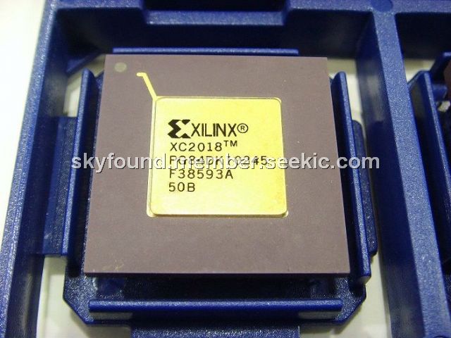
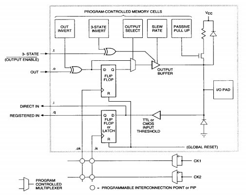
The XC2018-50PG84B is a Field-Programmable Gate Array (FPGA) provided the benefits of high-speed, custom CMOS VLSI while avoiding the Initial cost, time delay, and inherent risk of a conventional masked gate array. The XC2018-50PG84B is a performance-optimized relative of the industry-leading XC3000 family. While both families are bitstream and footprint compatible, the XC2018-50PG84B extends in-system performance to 80 MHz and beyond. The regular, flexible, re-programmable array architecture is composed of three standard types of programmable elements: a perimeter of Input/Output Blocks (IOBs), a core array of Configurable Logic Blocks (CLBs), and resources for interconnection. Xilinx FPGAs can be reprogrammed an unlimited number of times.
Parametrics
XC2018-50PG84B absolute maximum ratings: (1)Supply voltage relative to GND, Vcc: -0.5 to +7.0V; (2)Input voltage with respect to GND, ViN -0.5 to Vcc +0.5V; (3)Voltage applied to 3-state output, VTS: -0.5 to Vcc +0.5V; (4)Storage temperature (ambient), Tstg: -65 to +150℃; (5)Maximum soldering temperature (10 s @ 1/16 in), TSOL: +260℃; (6)Junction temperature plastic, Tj: +125℃; Junction temperature ceramic, Tj: +150℃.
Features
XC2018-50PG84B features: (1)100% architecture, pin out, and software compatible with XC3000 devices; (2)Ultra-High speed, up to twice that of XC3000-125; 50-80 MHz system clock rates-Flip-flop toggle rates of 190 to 270 MHz; Performance equivalent to 10 ns PALs in many applications; (3)Advanced Second-Generation Field-Programmable Gate Array, Programmable logic blocks, I/O blocks, and intorconnecl structure; Low-power, CMOS, static-memory technology; (4)Flexible Array Architecture; Compatible arrays, 2,000 to 13,500 gate logic complexity; Extensive register and I/O capability; Internal 3-state bus capabilities; Unlimited re-programmability; TTL or CMOS input thresholds; RaH-to-rail output swing; 2,000-V electrostatic-discharge input protection; 8-mA sink current per output; (5)Extensive Packaging Options, Common 84-pin plastic leaded chip carrier (PLCC) footprint; 44- to 223-pin plastic and ceramic surface mount and pin grid array packages; (6)Standard, off-the-shelf product availability, 100% factory pre-tested; (7)Complete XACT Development System, Schematic capture, automatic place and route; Logic and timing simulation Interactive design editor for design optimization; Library and user macros; Timing calculator; Standard PROM File Interlace.
Diagrams
 |
 XC2000 |
Other |
|
Data Sheet |
Negotiable |
|
||||
|
XC2000L |
Other |
|
Data Sheet |
Negotiable |
|
||||
|
XC2064 |
Other |
|
Data Sheet |
Negotiable |
|
||||